- 您现在的位置:买卖IC网 > Sheet目录39249 > LM4832MX/NOPB (NATIONAL SEMICONDUCTOR CORP) 2 CHANNEL(S), TONE CONTROL CIRCUIT, PDSO28
Application Information (Continued)
I
2C INTERFACE
The LM4832 uses a serial bus, which conforms to the I
2C
protocol, to control the chip’s functions with two wires: clock
and data. The clock line is uni-directional. The data line is bi-
directional(open-collector) with a pullup resistor (typically
10 k
).The maximum clock frequency specified by the I2C
standard is 400 kHz. In this discussion, the master is the
controlling microcontroller and the slave is the LM4832.
The I
2C address for the LM4832 is determined using the Ad-
dress Bit 1 and Address Bit 2 TTL/CMOS inputs on the chip.
The LM4832’s four possible I
2C chip addresses are of the
form 10000X
2X10 (binary), where the X2 and X1bits are de-
termined by the voltage levels at the Address Bit 2 and Ad-
dress Bit 1 pins, respectively. If the I
2C interface is used to
address a number of chips in a system and the LM4832’s
chip address can be changed to avoid address conflicts.
The timing diagram for the I
2C is shown in Figure 2. The data
is latched in on the stable high level of the clock and the data
line should be held high when not in use. The timing diagram
is broken up into six major sections:
The “start” signal is generated by lowering the data signal
while the clock signal is high. The start signal will alert all de-
vices attached to the I
2C bus to check the incoming address
against their own chip address.
The 8-bit chip address is sent next, most significant bit first.
Each address bit must be stable while the clock level is high.
After the last bit of the address is sent, the master checks for
the LM4832’s acknowledge. The master releases the data
line high (through a pullup resistor). Then the master sends
a clock pulse. If the LM4832 has received the address cor-
rectly, then it holds the data line low during the clock pulse.
If the data line is not low, then the master should send a
“stop” signal (discussed later) and abort the transfer.
The 8 bits of data are sent next, most significant bit first.
Each data bit should be valid while the clock level is stable
high.
After the data byte is sent, the master must generate another
acknowledge to see if the LM4832 received the data.
If the master has more data bytes to send to the LM4832,
then the master can repeat the previous two steps until all
data bytes have been sent.
The “stop” signal ends the transfer. To signal “stop”, the data
signal goes high while the clock signal is high.
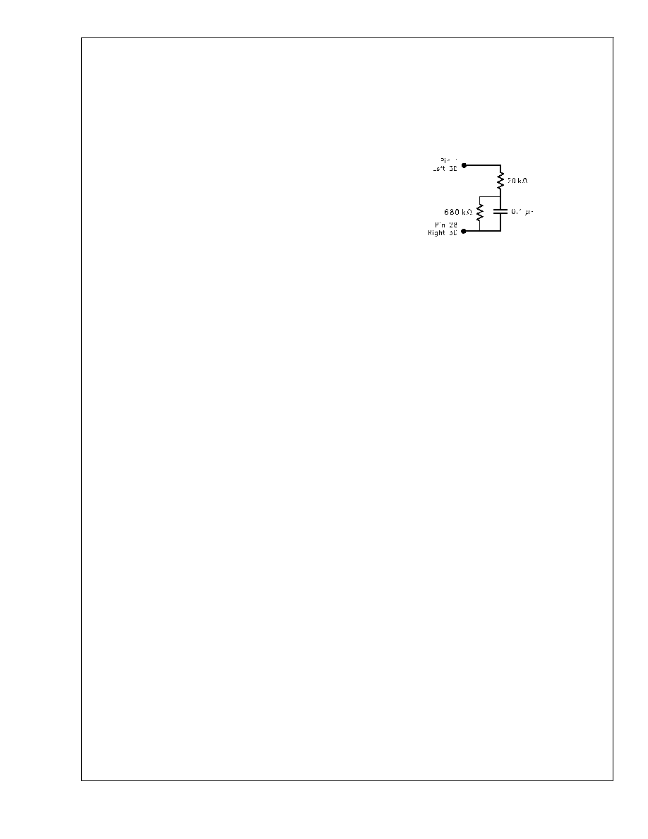
3D AUDIO ENHANCEMENT
The LM4832 has a 3D audio enhancement effect that helps
improve the apparent stereo channel separation when, be-
cause of cabinet or equipment limitations, the left and right
speakers are closer to each other than optimal.
An external RC network, shown in
Figure 3, is required to en-
able the effect. The amount of the effect is set by the 20 k
resistor. A 0.1 F capacitor is used to reduce the effect at fre-
quencies below 80 Hz. Decreasing the resistor size will
make the 3D effect more pronounced and decreasing the ca-
pacitor size will raise the cutoff frequency for the effect.
The 680 k
resistor across the 0.1 F capacitor reduces
switching noise by discharging the capacitor when the effect
is not in use.
TONE CONTROL RESPONSE
Bass and treble tone controls are included in the LM4832.
The tone controls use two external capacitors for each ste-
reo channel. Each has a corner frequency determined by the
value of C2 and C3 (see
Figure 4) and internal resistors in
the feedback loop of the internal tone amplifier.
Typically, C2 = C3 and for 100 Hz and 10 kHz corner fre-
quencies, C2 = C3 = 0.0082 F. Altering the ratio between
C2 and C3, changes the midrange gain. For example, if C2
= 2(C3), then the frequency response will be flat at 20 Hz
and 20 kHz, but will havea6dB peak at 1 kHz.
WithC=C2=C3, the treble turn-over frequency is nominally
f
TT = 1/(2πC(14 k))
and the bass turn-over frequency is nominally
f
BT = 1/(2πC(30.4 k)),
when maximum boost is chosen. The inflection points (the
frequencies where the boost or cut is within 3 dB of the final
value) are, for treble and bass respectively,
f
TI = 1/(2πC(1.9 k))
f
BI = 1/(2πC(169.6 k))
Increasing the values of C2 and C3 decreases the turnover
and inflection frequencies: i.e., the Tone Control Response
Curves shown in Typical Performance Section will shift left
when C2 and C3 are increased and shift right when C2 and
C3 are decreased. With C2 = C3 = 0.0082 F, 2 dB steps are
achieved at 100 Hz and 10 kHz. Changing C2 and C3 to
0.01 F shifts the 2 dB step frequency to 72 Hz and 8.3
kHz.If the tone control capacitors’ size is decreased these
frequencies will increase.With C2 = C3 = 0.0068 F the 2 dB
steps take place at 130 Hz and 11.2 kHz.
DS100014-28
FIGURE 5. 3D Effect Components
LM4832
www.national.com
14
发布紧急采购,3分钟左右您将得到回复。
相关PDF资料
LM4836MTX/NOPB
2 CHANNEL(S), TONE CONTROL CIRCUIT, PDSO28
LM4842MH/NOPB
2 CHANNEL(S), TONE CONTROL CIRCUIT, PDSO28
LM4842MT/NOPB
2 CHANNEL(S), TONE CONTROL CIRCUIT, PDSO28
LM4842LQ/NOPB
2 CHANNEL(S), TONE CONTROL CIRCUIT, QCC28
LM4849MH/NOPB
2 CHANNEL(S), VOLUME CONTROL CIRCUIT, PDSO28
LM4867MTE/NOPB
3 W, 2 CHANNEL, AUDIO AMPLIFIER, PDSO20
LM4867MT/NOPB
1.5 W, 2 CHANNEL, AUDIO AMPLIFIER, PDSO20
LM4867LQ/NOPB
3 W, 2 CHANNEL, AUDIO AMPLIFIER, PQCC24
相关代理商/技术参数
LM4832N
制造商:NSC 制造商全称:National Semiconductor 功能描述:Digitally Controlled Tone and Volume Circuit with Stereo Audio Power Amplifier, Microphone Preamp Stage and National 3D Sound
LM4832N/NOPB
功能描述:IC AMP AUDIO PWR .25W STER 28DIP RoHS:是 类别:集成电路 (IC) >> 线性 - 音頻放大器 系列:Boomer® 产品培训模块:Lead (SnPb) Finish for COTS
Obsolescence Mitigation Program 标准包装:2,500 系列:DirectDrive® 类型:H 类 输出类型:耳机,2-通道(立体声) 在某负载时最大输出功率 x 通道数量:35mW x 2 @ 16 欧姆 电源电压:1.62 V ~ 1.98 V 特点:I²C,麦克风,静音,短路保护,音量控制 安装类型:表面贴装 供应商设备封装:25-WLP(2.09x2.09) 封装/外壳:25-WFBGA,WLCSP 包装:带卷 (TR)
LM4834
制造商:NSC 制造商全称:National Semiconductor 功能描述:1.75W Audio Power Amplifier with DC Volume Control and Microphone Preamp
LM4834A E WAF
制造商:Texas Instruments 功能描述:
LM4834MS
制造商:Texas Instruments 功能描述:28 pin Boomer 1.75W Audio Power Amplifier with DC Volume Control and Microphone Preamp 47 per tube 制造商:Texas Instruments 功能描述:IC, AUDIO PWR AMP CLASS AB 1.75W SSOP-28, Amplifier Class:AB, No. of Channels:1,
LM4834MS/NOPB
功能描述:IC AMP AUDIO PWR 1.1W AB 28SSOP RoHS:是 类别:集成电路 (IC) >> 线性 - 音頻放大器 系列:Boomer® 产品培训模块:Lead (SnPb) Finish for COTS
Obsolescence Mitigation Program 标准包装:2,500 系列:DirectDrive® 类型:H 类 输出类型:耳机,2-通道(立体声) 在某负载时最大输出功率 x 通道数量:35mW x 2 @ 16 欧姆 电源电压:1.62 V ~ 1.98 V 特点:I²C,麦克风,静音,短路保护,音量控制 安装类型:表面贴装 供应商设备封装:25-WLP(2.09x2.09) 封装/外壳:25-WFBGA,WLCSP 包装:带卷 (TR)
LM4834MSX/NOPB
功能描述:IC AMP AUDIO PWR 1.1W AB 28SSOP RoHS:是 类别:集成电路 (IC) >> 线性 - 音頻放大器 系列:Boomer® 产品培训模块:Lead (SnPb) Finish for COTS
Obsolescence Mitigation Program 标准包装:2,500 系列:DirectDrive® 类型:H 类 输出类型:耳机,2-通道(立体声) 在某负载时最大输出功率 x 通道数量:35mW x 2 @ 16 欧姆 电源电压:1.62 V ~ 1.98 V 特点:I²C,麦克风,静音,短路保护,音量控制 安装类型:表面贴装 供应商设备封装:25-WLP(2.09x2.09) 封装/外壳:25-WFBGA,WLCSP 包装:带卷 (TR)
LM4835
制造商:NSC 制造商全称:National Semiconductor 功能描述:Stereo 2W Audio Power Amplifiers with DC Volume Control and Selectable Gain